Equipment of Mikrostrukturlabor (MSL)
The Mikrostrukturlabor (MSL) offers a wide array of fabrication and characterization tools as well as established process chains for complex micro- and nanostructures made form a wide array of materials. We are happy to assist with services as well as granting lab access for internal and external users who peruse more complex tasks requiring significant lab time.
If you are interested in any of our tools, processes, or similar, please do not hesitate contacting us
Lithography
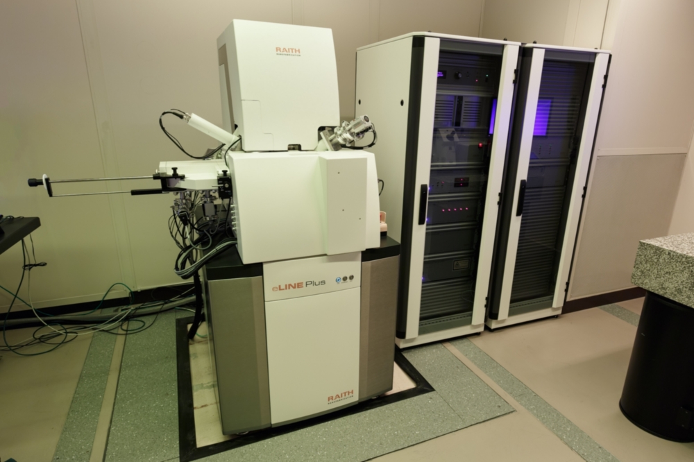
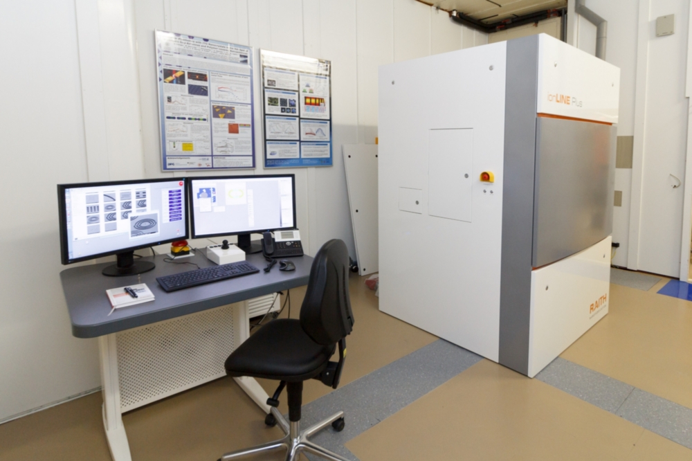
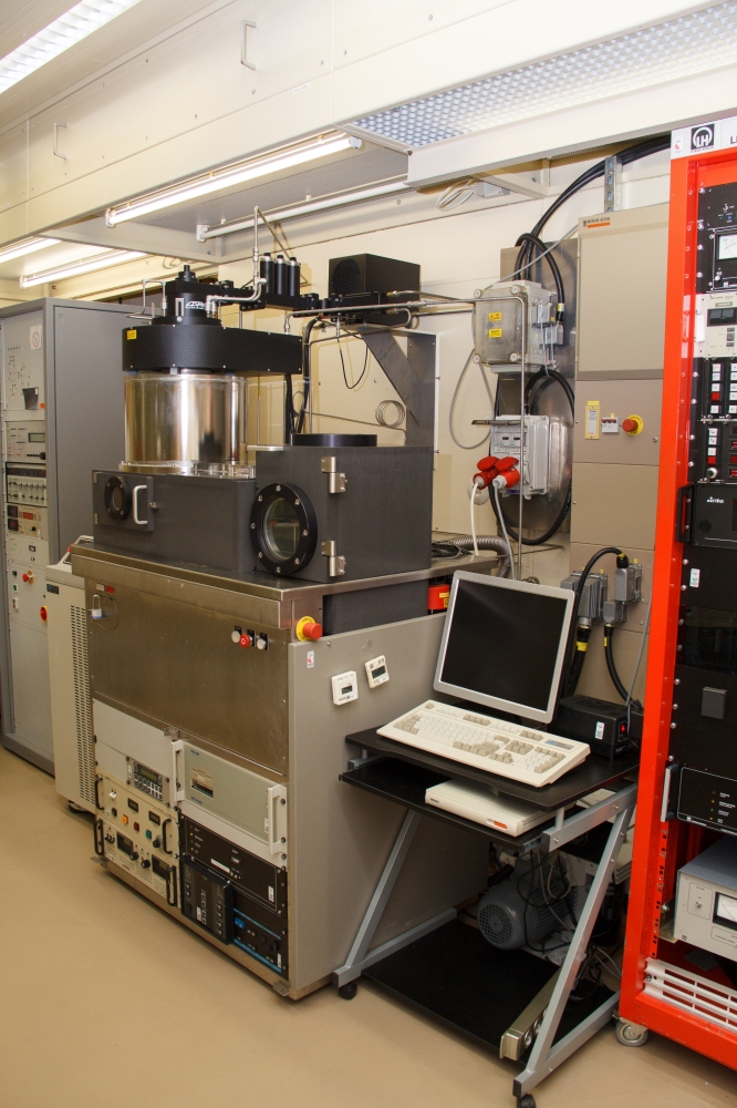
Positive and negative tone processes available, acceleration voltage up to 30kV, resolution 10nm, laser interferometer stage, stitching and overlay (30nm, mean+3s), high resolution-low current and low resolution-large current modes, electron beam induced deposition (EBID), fixed beam moving stage, nanomanipulators.
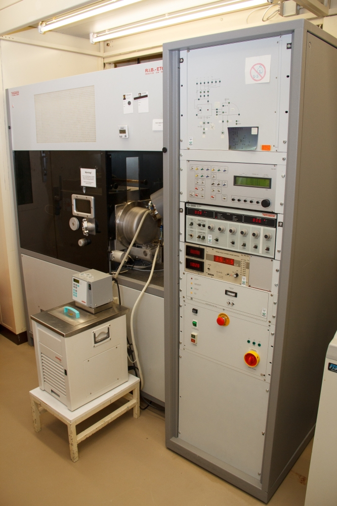
Direct milling of samples, acceleration voltage 35kV, ion implantation, ion species: Si+, Si++, Au+, Au++, laser interferometer stage, stitching and overlay (30nm, mean+3s), ion beam induced deposition (IBID), overlay processes with electron beam lithography possible.

- Nanoscribe Photonic Professional: Three dimensional structuring of resists, resolution ~100nm, two dimensional structuring also possible.
- Nanoscribe Quantum X: High-throughput tool
- Carl Süss mask aligner: Optical lithography, resolution ~300nm.
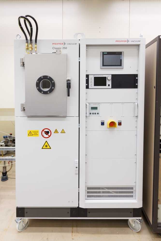
Thin Film deposition
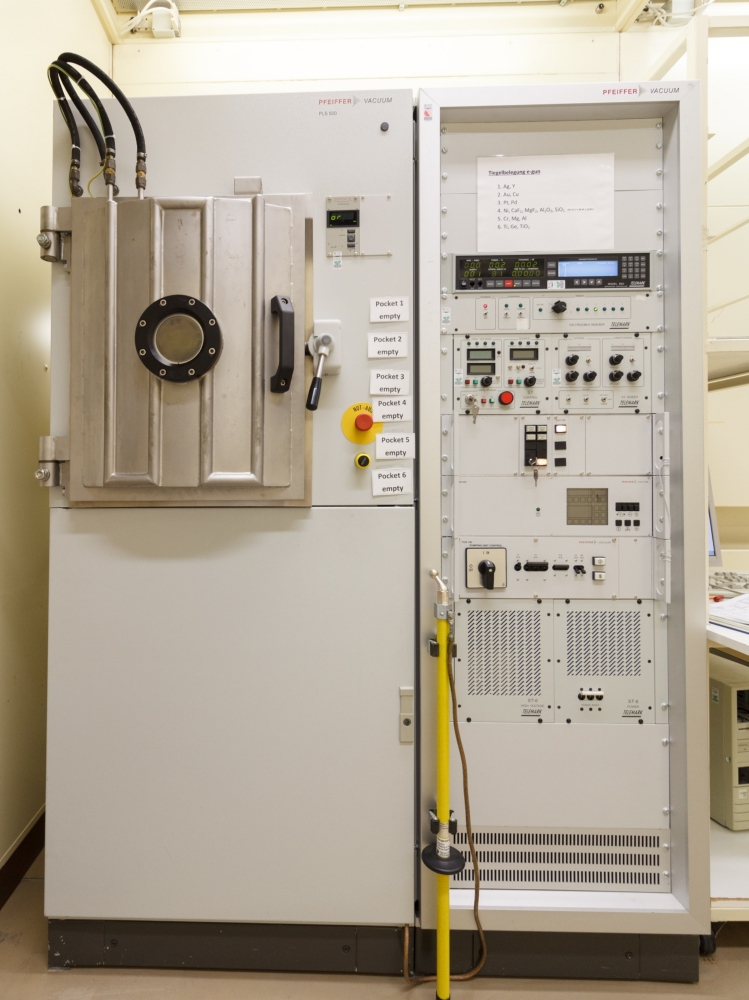
6 crucible electron beam evaporator, metals and dielectrics.
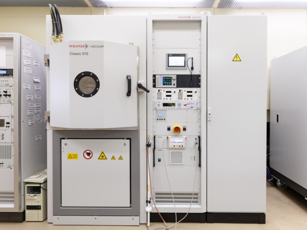
6 crucible electron beam evaporator, DC and RF sputtering, reactive Sputtering, sample holder can be in-situ tilted and rotated.
Thermal evaporator with two sources, source and sample shutter (evaporation of different thicknesses in the same run possible).
Thermal evaporator with three sources, samples sizes > 4’’ possible.
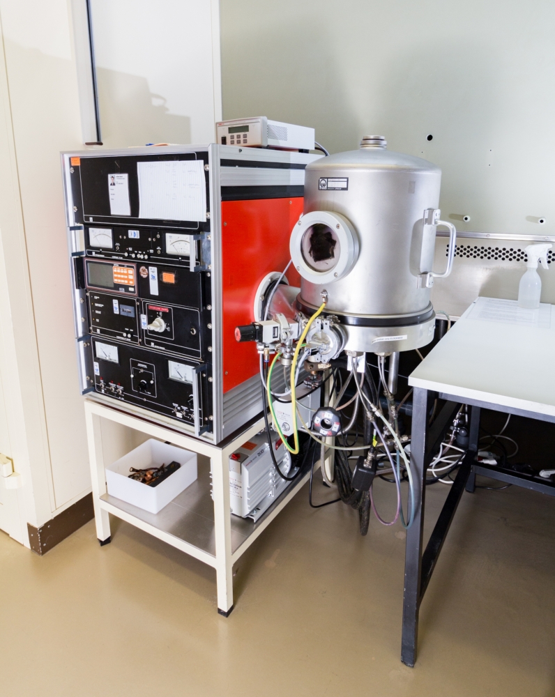
Thermal evaporator with four sources.
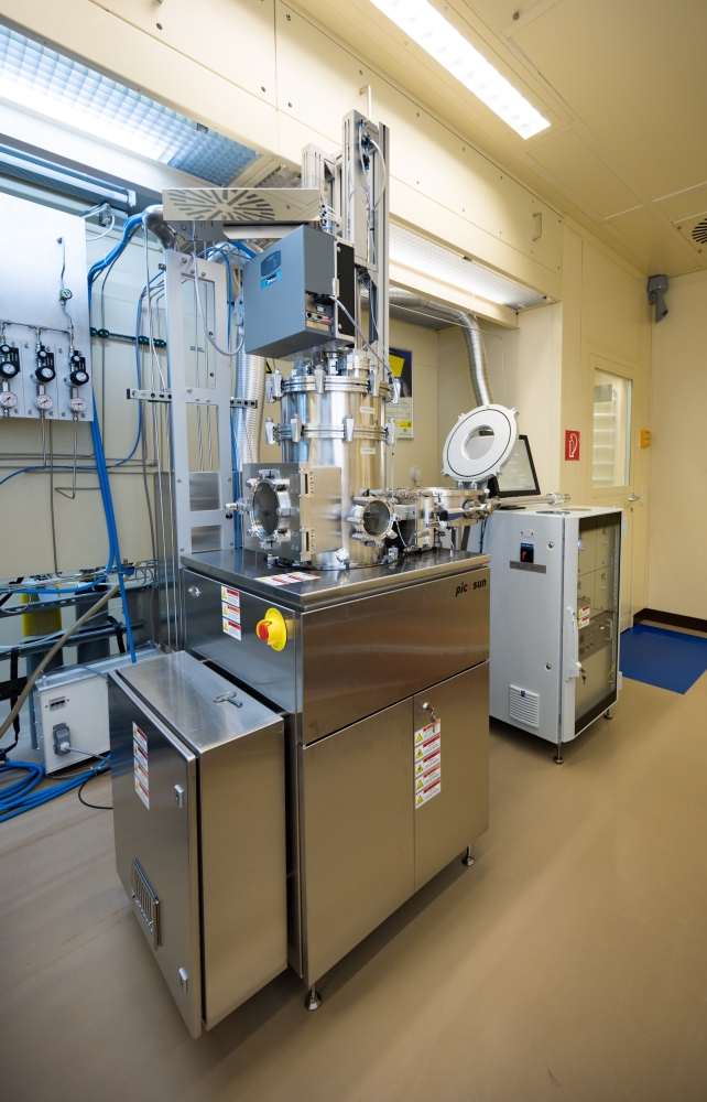
Picosun R200 Advanced Plasma: Conformal coatings /thermal as well as plasma enhanced) with high and low index materials: TiO2, SiO2, HfO2, Al2O3
Microscopy
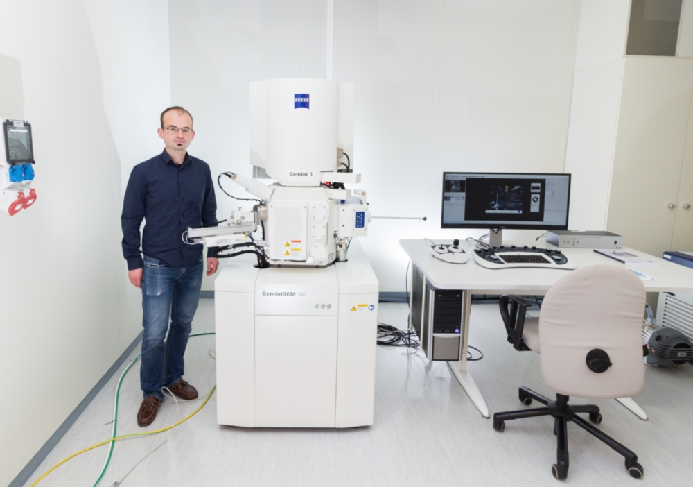
Zeiss SEM Gemini 560 with Oxford EDX.
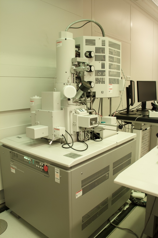
Hitachi S-4800: Acceleration voltage up to 30kV, SE, BSE, and YAG detectors, samples size up to 4’’, in-situ tilt and rotation, various sample holders.
- Veeco di CP-II
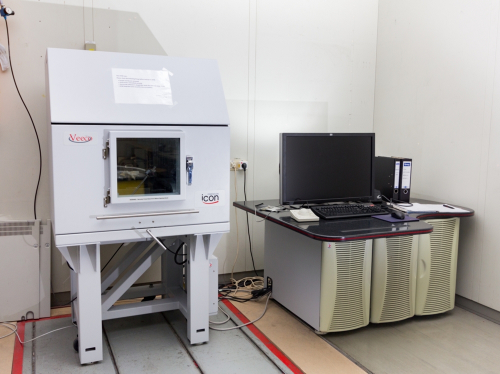
- Veeco Dimension Icon
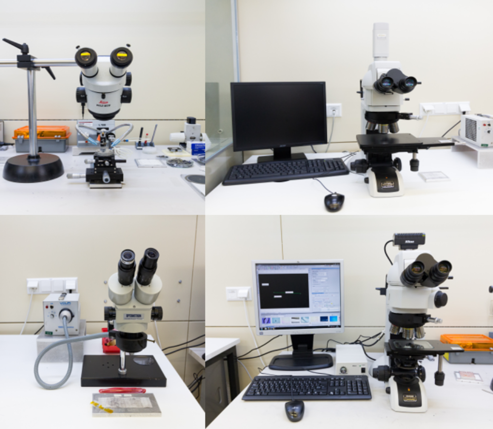
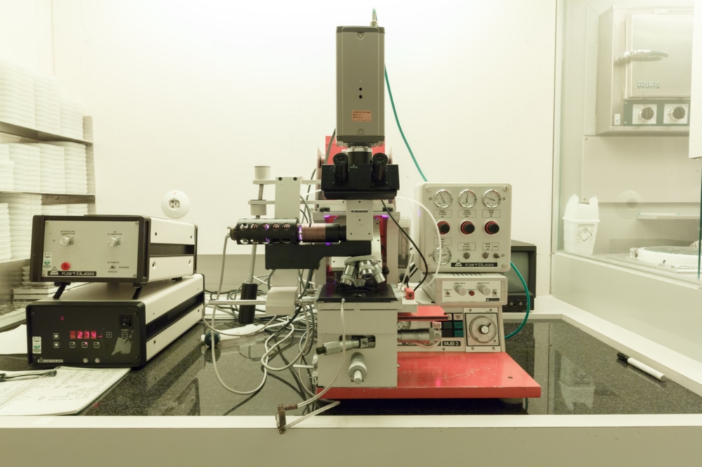
- Nikon LV100ND (2x): Darkfield and brightfield imaging, transmission and reflection, up to 100x
- Macroscopy
- Wafer Dicing
Dry Etching
Ar ion beam etching, theoretically all materials possible (depends on etching rates mask vs. material).
Available gases CHF3, CF4, Ar, O2, He
Available gases BCl3, SiCl4, Cl2, CH4, H2, CHF3, SF6, O2, Ar, He, N2
Profilometry

Thickness measurement with stylus.
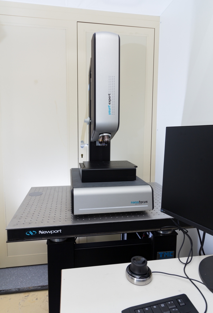
Confocal microscope, contact free, additional in-plane 2D information.
Wire Bonding

Ball- and wedgebing, Al and Au.
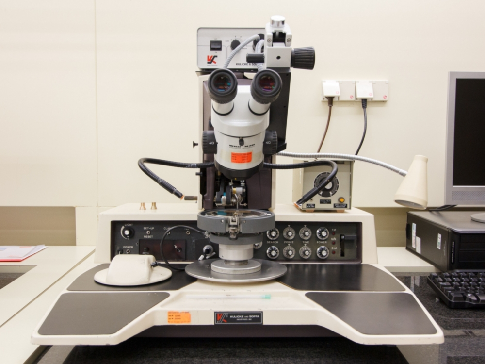
Wedge bonding, Au.
Miscellaneous

- Technics: O2 plasma (right)
- Diener Pico Standard: O2, H2 plasma (left)
Controlled environment (vacuum, gases), up to 500°C.

Up to 1100°C and up to 1650°C

Spin coating, precision hot plates (N2 flushed, pins), hot plates, ultra-sonic bathes, etching bathes, ovens.